Qualcomm HBC Silicon Passes Validation Ahead of 2027 AI250 Sampling
-

- by THEFLGHT,
- November 03, 2026
- in Artificial-Intelligence
Qualcomm HBC silicon has completed its first physical validation, with the company reporting a working memory read-write path and near-memory computations in its San Diego laboratory. The November 2 milestone moves High Bandwidth Compute from a proposed architecture toward integration in Qualcomm’s Dragonfly AI250 data-center accelerator.
The test does not mean a full AI250 card or rack is ready for customers. Qualcomm evaluated an early HBC stack with automated test equipment, while commercial sampling of the complete accelerator remains targeted for the first half of 2027.
The silicon update establishes four concrete engineering milestones:
- The complete memory path operated in physical silicon.
- Near-memory computations ran with randomized weights and activations.
- A related data-center product has taped out.
- Dragonfly AI250 sampling is planned for early 2027.
Related Coverage
Qualcomm HBC Silicon Completes Its First Physical Validation
Qualcomm’s official validation report says engineers exercised the full memory read-write path and computations at production-representative dimensions. The test used industry-standard automated equipment and randomized model weights and activations rather than relying only on design simulations.
The company says the electrical, thermal and physical foundations have been demonstrated through dedicated test vehicles. It has also qualified a wafer-to-wafer bonding process, built redundancy and remapping into the design, and developed methods for testing defects and interface failures.
A data-center product using the architecture has taped out, meaning its design was finalized for fabrication. Qualcomm also reports early progress bringing up a logic base bonded to DRAM tiers. Those steps reduce technical uncertainty, but they are not the same as validating a production accelerator under customer workloads.
Independent analysis from ServeTheHome says the test stack contained two DRAM layers, while the intended shipping product will use four. The publication also notes that thermal behavior remains a central challenge when active compute sits beneath stacked memory.
How HBC Targets the AI Inference Memory Bottleneck
Large-model inference repeatedly moves weights and cached data into compute units while generating tokens. When memory cannot supply that data quickly enough, adding more arithmetic capacity does not produce a proportional speed increase. The energy used to move data also becomes a major operating cost at data-center scale.
HBC places compute closer to stacked memory, allowing selected low-arithmetic operations to occur within the package. Qualcomm argues that shorter data paths can increase effective bandwidth and reduce the power spent moving information between memory and a separate processor.
The company says its measured first-generation silicon delivered roughly 18 times the bandwidth of external LPDDR5X and more than five times the bandwidth-per-watt of HBM4. These comparisons are Qualcomm’s laboratory measurements normalized to target conditions and published competing specifications, not independently audited system benchmarks.
The five-times efficiency result is slightly below Qualcomm’s earlier six-times design target. That difference is useful because it separates measured early silicon from the projections used when the architecture was announced. Final performance can still change with the four-layer stack, packaging, cooling, firmware and production yields.
Dragonfly AI250 Is the First Commercial HBC Test
Qualcomm plans to integrate HBC Gen 1 into Dragonfly AI250, its second-generation inference accelerator. The current product specification targets 133 terabytes per second of effective memory bandwidth and 768 gigabytes of memory per card, with support for large models and long context windows.
Those figures remain design claims until complete cards run reproducible workloads. AI250 is expected to sample in the first half of 2027, after which hyperscalers and server partners can evaluate throughput, latency, power, software compatibility and reliability outside Qualcomm’s lab.
The accelerator will also anchor the Dragonfly Rack, an open rack-scale inference system offered with air or direct-liquid cooling. Qualcomm is emphasizing token generation rather than training, positioning the platform for continuous reasoning, agents and other services that repeatedly decode model outputs.
This strategy puts memory economics at the center of Qualcomm’s challenge to established data-center accelerators. If HBC produces more useful tokens per watt and per dollar, cloud operators gain another option for serving models. If yields, thermals or software integration fall short, high laboratory bandwidth will not guarantee competitive deployment.
Production Yield and Independent Benchmarks Are the Next Gates
The validation is important because physical silicon exposed the complete path and near-memory compute functions to real test equipment. It also shows that Qualcomm’s multi-year program has moved beyond diagrams. However, the company has not published raw test data, full thermal results or an outside verification of its bandwidth comparisons.
The next evidence should come from four-layer stacks, full AI250 cards and rack-level measurements on disclosed models. Buyers will need tokens per second, tail latency, watts, memory capacity, utilization and total cost across comparable systems, along with failure rates and manufacturing yields.
Software will matter as much as packaging. Qualcomm must make common models and serving frameworks run reliably across its inference suite, networking and rack management tools. An accelerator with unusual memory behavior can create value only if operators can deploy workloads without excessive conversion or engineering effort.
For now, the verified event is narrower than a product launch: Qualcomm has demonstrated a functioning first-generation HBC stack and advanced the design toward AI250 integration. The first-half 2027 sampling window will determine whether that memory experiment becomes a deployable alternative for large-scale inference.
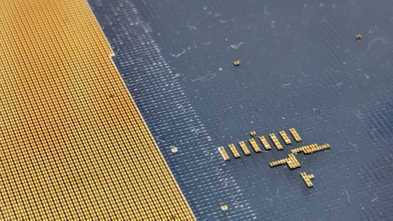
Illustrative photo: a semiconductor wafer photographed by Syced, via Wikimedia Commons. Released under CC0 1.0. Cropped and resized to 16:9; the image does not show Qualcomm’s HBC test silicon.






0 Comments:
Leave a Reply