Google Launches TPU 8tx and TPU 8i Max for Secure AI
-

- by THEFLGHT,
- November 09, 2026
- in Artificial-Intelligence
Google launches TPU 8tx for confidential AI inference and TPU 8i Max for workloads that need unusually large memory capacity. The November 9 announcement expands Google's eighth-generation accelerator portfolio to four systems.
The products are specialized system configurations rather than entirely new chip architectures. Google rearranged the processors, host CPUs, memory, networking and packaging around its existing TPU 8t and TPU 8i silicon to address regulated data and million-token context workloads.
The two TPU systems divide the new workloads clearly:
- TPU 8tx protects data and model weights during processing.
- TPU 8i Max combines two inference chips in one package.
- 8tx targets regulated enterprises and government users.
- 8i Max targets long-context agents and dense racks.
Google Launches TPU 8tx for Confidential Inference
Google says TPU 8tx uses the same accelerator silicon as TPU 8t and pairs it with fifth-generation AMD EPYC host processors. Its distinguishing feature is hardware-level confidential computing for models and sensitive data that must remain isolated while actively in use.
Encryption at rest protects stored information, while encryption in transit protects data moving across a network. Confidential computing addresses the harder stage when a processor needs access to usable data in memory, where conventional systems normally expose plaintext to the computing environment.
Google positions the system for banks, public agencies and other organizations that need to run proprietary models or agents beside regulated data. The company says teams can fine-tune models, perform distillation and train agents through reinforcement learning without moving their information between separate clusters.
TPU 8tx also adopts Google's low-latency Boardfly network. Google claims up to twice the speed of TPU 8t for the targeted inference workload with a near-zero performance penalty from the security controls. That comparison remains a vendor claim, and Google has not published independent workload results for 8tx.
TPU 8i Max Doubles Compute, SRAM and HBM Bandwidth
TPU 8i Max addresses memory pressure rather than confidential processing. Google combines two TPU 8i chips in a single package, doubling compute, on-chip SRAM and high-bandwidth-memory throughput compared with one 8i package.
The dual-chip design is intended for coding agents that examine entire repositories, models processing hours of video and other applications with large working contexts. More memory bandwidth can keep processors supplied with model state and cached context instead of waiting for data to arrive.
Google also says the package doubles accelerator silicon inside the existing rack footprint. That increases compute density per square foot, but the announcement does not provide power consumption, cooling requirements or total rack cost, so buyers cannot yet compare density with operating expense.
Data Center Dynamics independently confirmed that 8tx and 8i Max are systems built around earlier eighth-generation designs. This distinction avoids treating a packaging and infrastructure release as two completely new processor generations.
Four Eighth-Generation TPUs Split Training and Inference
Google introduced TPU 8t for large-scale model training and TPU 8i for low-latency reasoning earlier in 2026. The company now describes 8tx as the secure variant of its training-class system and 8i Max as a high-memory, high-density extension of the inference platform.
The four-system portfolio lets Google tune infrastructure around distinct workloads without waiting for another silicon design cycle. The strategy uses common accelerator foundations while changing host processors, memory, packaging and network topology for training, real-time reasoning, confidential execution or massive contexts.
Google says it has nearly 100 TPU customers, including frontier laboratories, trading firms, retailers and universities. Reuters reported that the release strengthens Google's effort to sell custom accelerators through Google Cloud and compete for workloads that often run on NVIDIA GPUs.
Software remains a major part of that competition. Google is opening more of its TPU stack to PyTorch and popular inference frameworks, while its TPU Sync software moves model state among accelerator memory, host memory, shared storage and the data-center network.
Pricing and Deployment Dates Remain Undisclosed
Google's launch post does not list pricing, supported regions or a general-availability date for either new system. It also omits chip clock rates, absolute memory capacity, power draw and benchmark methodology detailed enough for independent price-performance comparisons.
Those gaps matter because confidential computing can impose operational constraints, while a dual-chip package can increase power and cooling demands even when it improves density. Enterprises will need full system specifications and representative application tests before deciding whether the specialized hardware lowers total inference cost.
The strongest immediate claim is architectural rather than commercial: Google has created two deployment profiles from existing TPU silicon. TPU 8tx prioritizes data protection during computation, while TPU 8i Max concentrates memory and processing capacity for agents that maintain very large working contexts.
The release therefore expands the range of problems Google can address with its own accelerators without proving that either system outperforms competing GPUs for every workload. Availability, pricing and customer deployments will determine whether specialization becomes a material advantage outside Google's internal infrastructure.
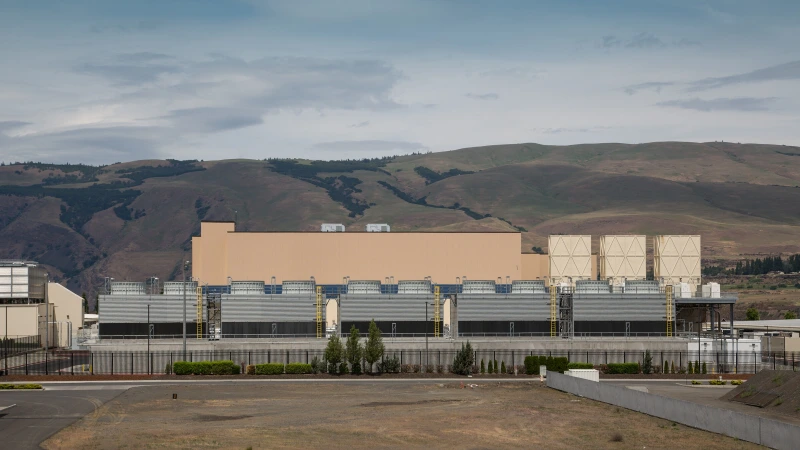
Feature image: Google's data center in The Dalles, Oregon, photographed by Tony Webster, via Wikimedia Commons under CC BY 2.0. Cropped to 16:9. The photograph shows a Google data center, not the TPU 8tx or TPU 8i Max systems.






0 Comments:
Leave a Reply